


反激开关电源反馈环路计算过程
输出电压调节1. Vout increases REF terminal voltage of TL431 TL431 cathode current optocoupler LED current optocoupler transistor current PWM chip FB pin voltage duty cycle decreases Vout falls back.
2、Vout减小反向调整,占空比增大。
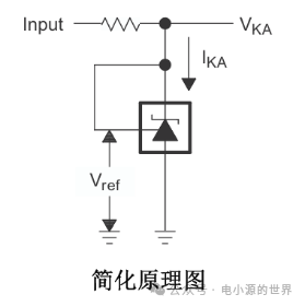
一、TL431部分参数计算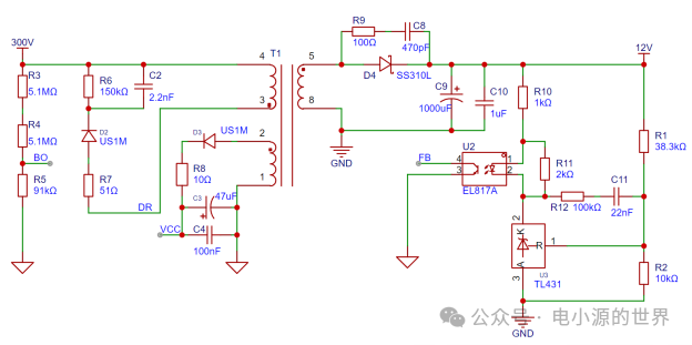
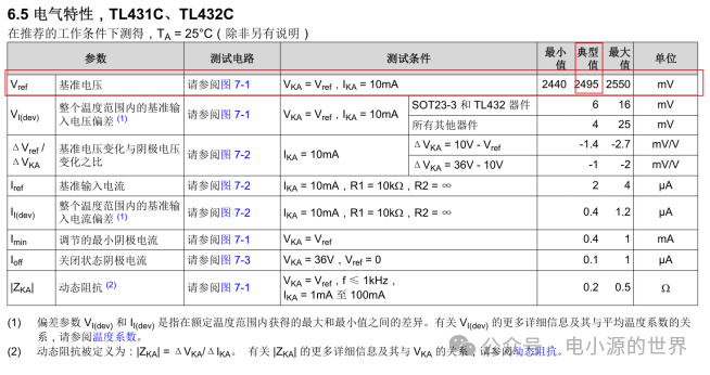
1.分压电阻(R1、R2)计算(1) TL431 通过分压电阻检测输出电压,当REF 端电压达到参考电压(典型值2.495V)时导通。
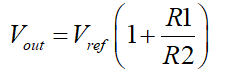
(2)公式:
(3)设计步骤:
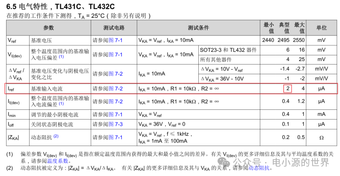
Usually the current flowing through the resistor R2 is set to be 100 times greater than the TL431 control electrode current (2A), so that it can work stably, that is:
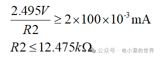
设定目标输出电压(如12V),选择R2(一般为10k),计算R1:
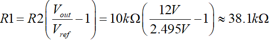
实际标称值为38.3k。
2.阴极电阻Rka设计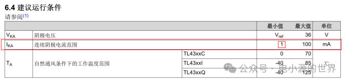
(1)确保TL431阴极电流Ika1mA以避免工作不稳定,Vka范围2.5V-36V,这样TL431才能正常工作: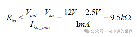
(实际取1k-5k,留余量)
二、光耦参数设计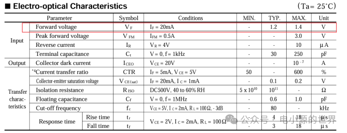
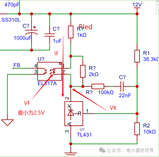
1.LED光敏二极管电流IF(1) The optocoupler primary LED photodiode current IF needs to meet the CTR (current transfer ratio) requirements:
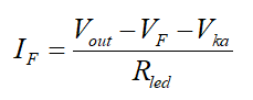
Among them: (VF is the LED forward voltage drop, about 1.2V)
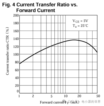
在5-20mA时,光耦的电流传输比比较稳定,即5mA
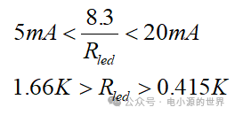
这里取1K
2.计算电阻R3的值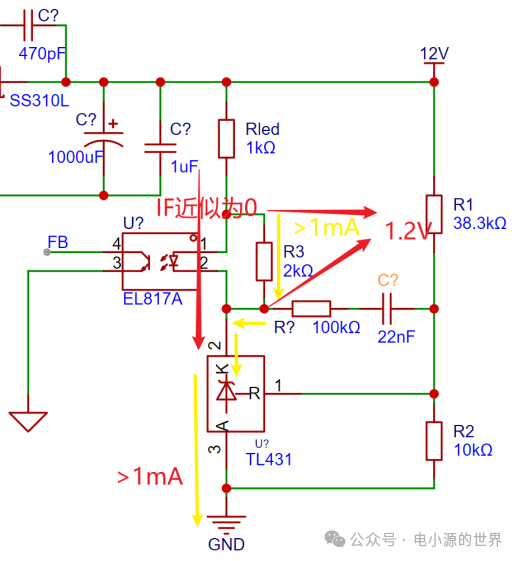
(1) The role of R3 is to provide a certain current (1mA) through R3 when the photodiode of the optocoupler is turned off to ensure the stability of TL431 (that is, to ensure that TL431 is always in working condition).
(2)当光电二极管接近截止状态时,光电二极管两端电压为1.2V。 See the screenshot in the manual above, which is the voltage across the resistor R3.此时
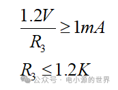
根据这里的计算,电阻应该小于1.2K,但大多数电路设计选择1.2K以上,也是可以工作的。但是这里为什么暂时还不清楚?希望有知道的能解答一下3.补偿网络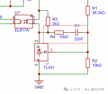
(1) Add an RC network (such as R4=10k, C1=22nF) to the REF end of TL431 or the secondary side of the optocoupler to stabilize the loop and compensate for the phase (usually 45 degrees) (it is not understandable here yet, and will be supplemented by subsequent learning).
(2)下面对AI进行解释
4.为什么需要补偿?(1)开关电源的固有问题 Phase lag: There are multiple poles in the power stage (MOSFET + transformer + diode) (such as the double poles of the output LC filter), resulting in a sharp drop in phase in the high frequency band.
Gain fluctuation: When the load changes, the open-loop gain may exceed 0dB, causing oscillation.
(2)TL431+光耦引入的延迟TL431: The error amplifier itself has about 60 phase lag (bandwidth 1-2kHz)
Optocoupler: PC817 and other devices add 20-40 phase delay (caused by CTR nonlinearity)
(3)不补偿的后果 输出电压振荡(表现为纹波增大)
Poor load transient response (recovery time is too long)
It may even cause the system to be completely unstable (continuous oscillation)
5.补偿网络的核心作用By adding RC network, realize:
(1) Phase compensation: Provide sufficient phase margin (45) at the crossover frequency (usually 1/10 of the switching frequency)
(2) Gain shaping: lower the high-frequency gain to avoid the rapid phase drop zone above 0dB